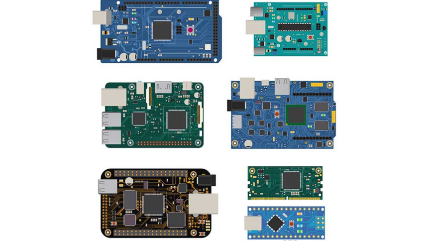
Picking the right components for your printed circuit board (PCB) is crucial for a successful design. There are several vital factors to bear in mind. Without a doubt, the following tips will guide you towards a high-quality PCB that satisfies your clients’ needs and specifications.
1. Choose Components at the Design Stage
The design phase is the optimal time to select components, as your design will dictate which parts are suitable. Conversely, the components available in the market will also influence your PCB design choices.
Therefore, choose a design that accommodates the physical dimensions and other characteristics of the components you intend to use. These include resistors, capacitors, transistors, and other essential parts.
You might establish new design goals – compact, power-efficient, or budget-friendly – or you might adapt a prior design. Following this tip will shed light on other aspects of the design process, including component selection.
2. Carefully Consider Component Footprint Decisions
As a PCB designer, you must choose footprints and land patterns that provide a solid base for your components. Make sure the footprint is compatible with the land pattern. Referencing the datasheet and utilizing its numerical guides for placement is crucial.
Ignoring the datasheet will likely result in an incorrect footprint, which can trigger numerous design problems.
3. Implement Proper Grounding Techniques
Ground planes are vital parts of any PCB and should include numerous bypass capacitors. When correctly placed near an integrated circuit (IC) pin, these capacitors facilitate smooth circuit operation and enable rapid performance.
These capacitors are critical, so pay attention to their size and frequency ratings. Prioritize good grounding practices throughout your PCB design.
4. Separate Leaded and Lead-Free Components
When selecting components, clearly differentiate lead-free parts from leaded ones to ensure a lead-free assembly. If a component’s lead status is not specified, it’s crucial to label it as lead-free. However, this is only recommended if leaded solder is unavoidable for the project.
Do not make this substitution without informing the client, as there are differences between leaded and lead-free components. For instance, government platform motherboards necessitate leaded solder.
5. Assign Footprints to Virtual Parts
Virtual parts represent ground and power signals. These virtual parts must be considered during the schematic design process. Their role in PCB design is indisputable.
Gain a better grasp of your PCB assembly’s virtual parts by cross-referencing with the Bill of Materials (BOM), which lists all components, including virtual ones.
The best practice is to assign footprints to the virtual parts and give them functions according to the BOM to optimize your PCB design.
6. Ensure Complete BOM Data
Another crucial aspect is the completeness of your Bill of Materials. You can reference the BOM report for the necessary information. Next, review and fill in the manufacturer’s details for each part before moving to the PCB layout stage.
A comprehensive BOM helps PCB manufacturers work faster and troubleshoot any issues more effectively.
7. Sort Reference Designators
Reference designators (RDs) are part of the BOM and specify the function and location of each component.
Sorting reference designators helps to organize the BOM’s content. For efficient workflow, ensure your reference designators are numbered sequentially for ease of review.
Remember, your reference designators must match the BOM data and be finalized before PCB layout.
8. Check Spare Gates
For a properly functioning PCB, inspect any unused gates. These are important because you want to connect inputs to signals to avoid floating pins.
To enhance PCB functionality and clarity, each spare gate in the schematic should be properly terminated to assist team members in understanding and operating the board. The component symbols for PCB layout, which are ultimately printed on the board, are important during assembly and must be placed correctly, particularly when dealing with unconnected inputs.
9. Consider Both Top and Bottom Sides of the PCB
Take into account the PCB’s housing. Pay attention to the height of components on both the top and bottom sides to ensure they fit within the enclosure. Also, consider the PCB’s perimeter and how to design it for easy handling and portability.
Remember, some components have height restrictions, so ensure your choices are compatible.
Summary
The aforementioned points are vital considerations for any PCB designer aiming to create exceptional PCBs. By following these tips, you will produce an elegant PCB that meets your needs or those of your clients.
I believe you now have a deeper understanding of PCB component selection. For further reading, please visit WellPCB. We have a decade of experience in PCB manufacturing and are ready to assist you with solutions and quality service. Don’t wait! Browse our circuit board selection – you might be surprised by what you find. Whether you’re in the market for a single-sided, double-sided, or any other PCB type, please contact us!
Lynn Martelli is an editor at Readability. She received her MFA in Creative Writing from Antioch University and has worked as an editor for over 10 years. Lynn has edited a wide variety of books, including fiction, non-fiction, memoirs, and more. In her free time, Lynn enjoys reading, writing, and spending time with her family and friends.